Table of Contents
Introduction to Scanning Electron Microscope (SEM)
The scanning electron microscope (SEM) is a highly advanced imaging technology used extensively in scientific research to examine the surface details of specimens at a microscopic level. Unlike traditional optical microscopes, SEMs utilize a focused beam of electrons to produce high-resolution images, allowing for the observation of fine surface structures that are otherwise invisible to the naked eye. This technology has revolutionized various fields, including materials science, biology, and nanotechnology, by providing unparalleled insights into the micro-world.
Scanning Electron Microscope (SEM)
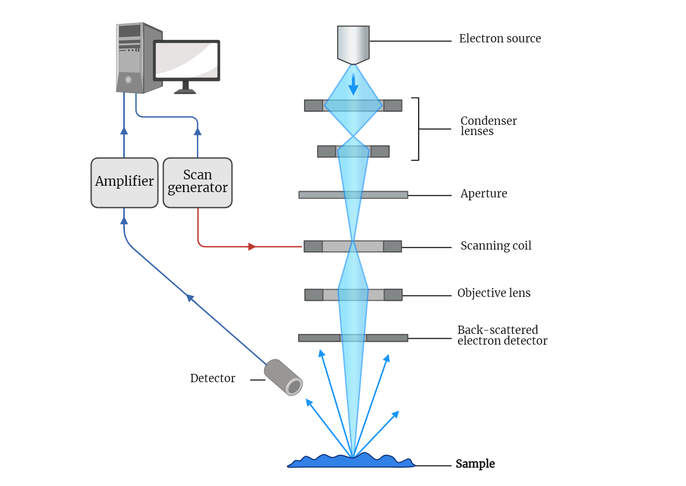
- Electron Gun and Magnetic Lenses: The SEM begins with the electron gun, which produces electrons that are crucial for imaging. These electrons are directed and focused by a series of magnetic lenses. The precision of these magnetic lenses ensures that the electron beam remains tightly focused on the specimen, allowing for high-resolution imaging.
- Scanning the Surface: Once the electrons are focused, they are systematically scanned across the specimen surface in a raster pattern. This movement is controlled by deflection or scanning coils. By moving the beam in this manner, the SEM can cover the entire surface of the specimen, collecting data from every point it scans.
- Image Formation: As the electron beam interacts with the specimen, it generates secondary electrons. The number of secondary electrons emitted at each scanned point is recorded and used to form a detailed, two-dimensional image of the specimen’s surface. This process allows scientists to observe minute details that are not visible with traditional optical microscopes.
Electron Detection
- Secondary Electron Detector: SEMs are equipped with detectors that specifically attract low-energy secondary electrons (with energies less than 50 eV). The detector is biased with a positive potential, which helps in attracting these electrons. Secondary electrons provide detailed information about the specimen’s surface topology, revealing fine surface details and textures.
- Backscattered Electron Detector: In addition to secondary electron detectors, SEMs also feature detectors for backscattered electrons. These detectors are not biased, as the high-energy backscattered electrons do not require additional attraction. Backscattered electrons originate from deeper within the specimen and can reveal information about its composition. Materials with higher atomic numbers scatter more electrons, resulting in brighter images. This makes backscattered electrons useful for distinguishing different elements within the sample.
Sample Preparation for SEM
- Fixation of Specimens: Preparing a specimen for SEM analysis involves several steps, starting with fixation. This step is crucial for biological specimens, which are not naturally dry. Fixation preserves the structural features of the specimen and can be achieved through chemical methods, such as using glutaraldehyde, or physical methods, like cryofixation in liquid nitrogen.
- Dehydration: After fixation, the specimen must be dehydrated to remove all water content. This is typically done by gradually exposing the specimen to an increasing gradient of ethanol, culminating in 100% ethanol. This step is essential to prevent structural damage that can occur due to dehydration.
- Drying: The dehydrated specimen is then dried using the critical point drying method. This technique ensures that the specimen retains its structural integrity without collapsing, which can happen if conventional drying methods are used.
- Coating with Conductive Material: The final step in sample preparation is coating the dried specimen with a conductive material, usually gold. This coating enhances the emission of secondary electrons and ensures that the surface is conductive, which is necessary for clear imaging. The conductive coating also helps in preventing the accumulation of static charge on the specimen’s surface during electron beam scanning.
Conclusion
The scanning electron microscope (SEM) is an indispensable tool in modern scientific research, providing exceptional detail and resolution in imaging specimen surfaces. By utilizing a focused electron beam and various detectors, SEMs can reveal intricate surface topologies and compositional information that are critical for advancements in numerous scientific fields. Proper sample preparation, including fixation, dehydration, drying, and coating, is essential to ensure high-quality imaging. The development and use of SEM technology continue to push the boundaries of our understanding of the microscopic world.
