Table of Contents
Introduction to Scanning Electron Microscope (SEM):
A scanning electron microscope (SEM) is an instrument that uses a beam of electrons to produce high-resolution images of a sample surface. It is an essential tool for many fields of science and technology, including materials science, biology, and geology.
Discovery of Scanning Electron Microscope (SEM):
The scanning electron microscope was first developed in the early 1930s by Max Knoll and Ernst Ruska. They were awarded the Nobel Prize in Physics in 1986 for their work in developing the SEM.
Principal of Scanning Electron Microscope (SEM):
- The SEM works by using a beam of electrons to scan a sample surface.
- The electrons interact with the atoms of the sample and produce a variety of signals, including secondary electrons, backscattered electrons, and x-rays.
- These signals are then used to create an image of the sample surface.
Components:
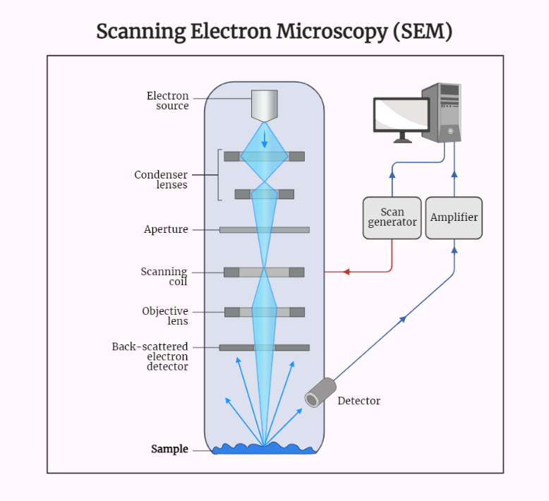
- The main components of a SEM include the electron gun, the column, the specimen stage, and the detector.
- The electron gun produces the electron beam that is used to scan the sample surface.
- The column is used to focus and control the electron beam.
- The specimen stage holds the sample in place during the scan.
- The detector is used to detect and measure the signals produced by the electron-sample interactions.
Steps:
- The first step in using a SEM is to prepare the sample. This can involve cleaning, coating, or cutting the sample.
- Next, the sample is placed on the specimen stage and the electron gun is turned on.
- The electron beam is then directed at the sample surface and the detector measures the signals produced by the electron-sample interactions.
- These signals are then used to create an image of the sample surface.
Applications:
- SEMs are used in a wide variety of fields, including materials science, biology, geology, and semiconductor manufacturing.
- They are used to study the structure and composition of materials, to examine biological samples, and to analyze geological samples.
- They are also used in semiconductor manufacturing to inspect and analyze the surface of semiconductor wafers.
The working principle of a SEM
- Electron Gun: The SEM starts by producing a beam of electrons using an electron gun. This beam is made up of a large number of electrons that are emitted at high speeds.
- Column: The electron beam is then directed through the column, which is used to focus and control the beam. The column contains a series of lenses and electromagnetic fields that are used to shape and direct the beam.
- Sample Stage: The sample to be examined is placed on the specimen stage. The stage is used to hold the sample in place during the scan and can also be used to move the sample in order to scan different areas.
- Electron-Sample Interaction: The electron beam is then directed at the sample surface. As the electrons interact with the atoms of the sample, they produce a variety of signals, including secondary electrons, backscattered electrons, and x-rays.
- Detector: The detector is used to detect and measure the signals produced by the electron-sample interactions. The detector is typically located behind the sample stage and can be used to measure the number of electrons, the energy of the electrons, and the position of the electrons.
- Image Creation: The signals measured by the detector are then used to create an image of the sample surface. This image can be viewed on a computer screen or can be saved for later analysis.
- Image Analysis: The image is then analyzed by the user. They can observe the surface of the sample, and can infer from the image about the sample’s structure, composition and other information.
Conclusion:
The scanning electron microscope is an essential tool for many fields of science and technology. Its ability to produce high-resolution images of a sample surface has led to many important discoveries and advancements in a wide variety of fields.
